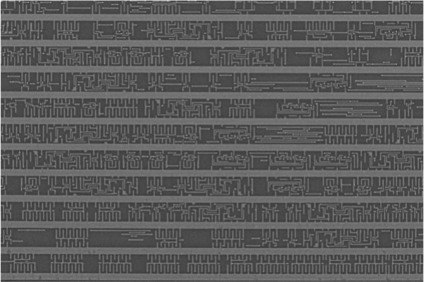
Scanning Electron Microscopy (SEM)
Scanning Electron Microscopy (SEM) provides high-resolution and high-depth-of-field images of the sample surface and near-surface. SEM is one of the most widely used analytical tools, due to the extremely detailed images it can quickly provide. Coupled to an auxiliary Energy Dispersive X-ray Spectroscopy (EDS) detector, SEM also offers elemental identification of nearly the entire periodic table.
Chip Campass Lab uses SEM analysis in cases where optical microscopy cannot provide sufficient image resolution or high enough magnification. The SEM also excels in producing detailed surface topography images. Applications include failure analysis, dimensional analysis, process characterization, reverse engineering and particle identification.